The Basics of PCB Design
PCB design is the process of creating a custom electronic circuit board. PCB design involves a number of different steps, including creating a schematic diagram for your circuit, designing the PCB layout, and finalizing the design for manufacturing. In this section, we’ll explore the basics of PCB design and what you need to know to get started.
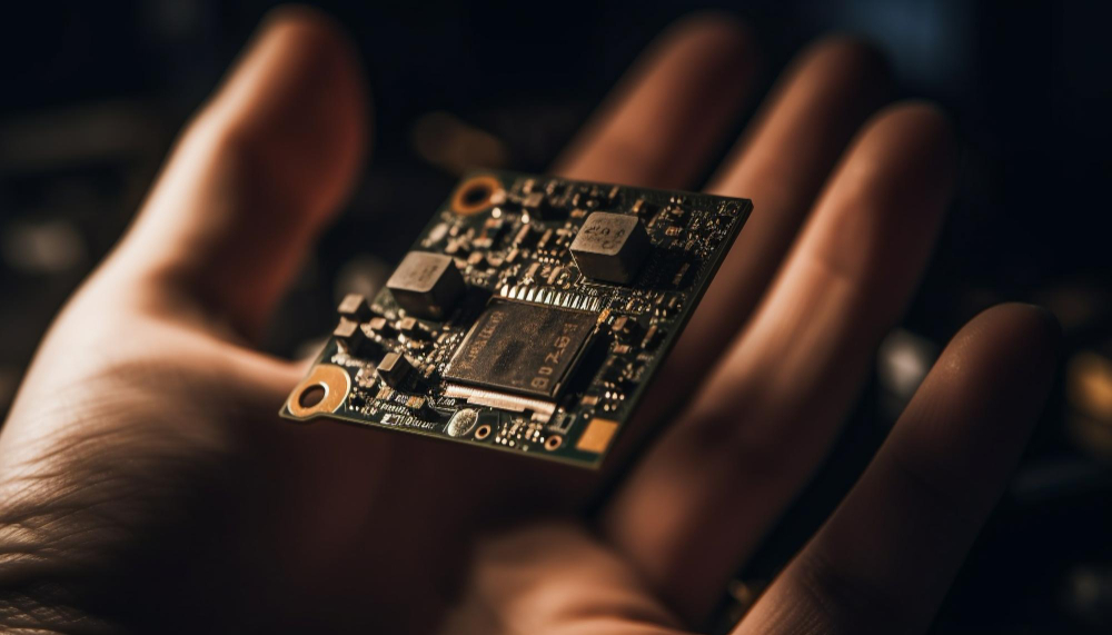
Components of a PCB
- Design Considerations
- Software Tools for PCB Design
- Creating a Schematic Diagram
- PCB Layout Design
- Finalizing the Design and Manufacturing the PCB
Solder Paste Application
Basic Information about SMT Components
- Resistors
- Capacitors
- Diodes
- ICs
Solder Paste Application
The solder paste is applied to the surface of the PCB through the screen printer. This ensures that the components stick to the board as they go through the production process.
Surface Mount Technology
Pick and Place machine picks components from the reels and places it in the exact position on the PCB.
Reflow Oven
Reflow oven is used for melting the solder paste on the board to form an electrical and
mechanical connection between the components and the PCB.
Wave Soldering
The PCB is transferred to the wave soldering machine, where the through-hole components on the opposite side of the PCB are soldered to ensure the strongest electrical connection with the PCB
Inspection Machine
An inspection machine ensures that the components are correctly placed and the solder joints are properly formed. It helps in detecting defects such as missing components, orientation issues, bridging between tiny components and solder voids.
Master the Art of SMT:
Spark your Skills in Production!
Future Applications
Want to master the art of SMT production? Join our training and unlock the secrets of efficient and precise electronic manufacturing. From soldering techniques to component placement, we’ve got you covered. Elevate your skills and become an SMT production pro in no time. Get ready to revolutionize the manufacturing game!